Hi All,
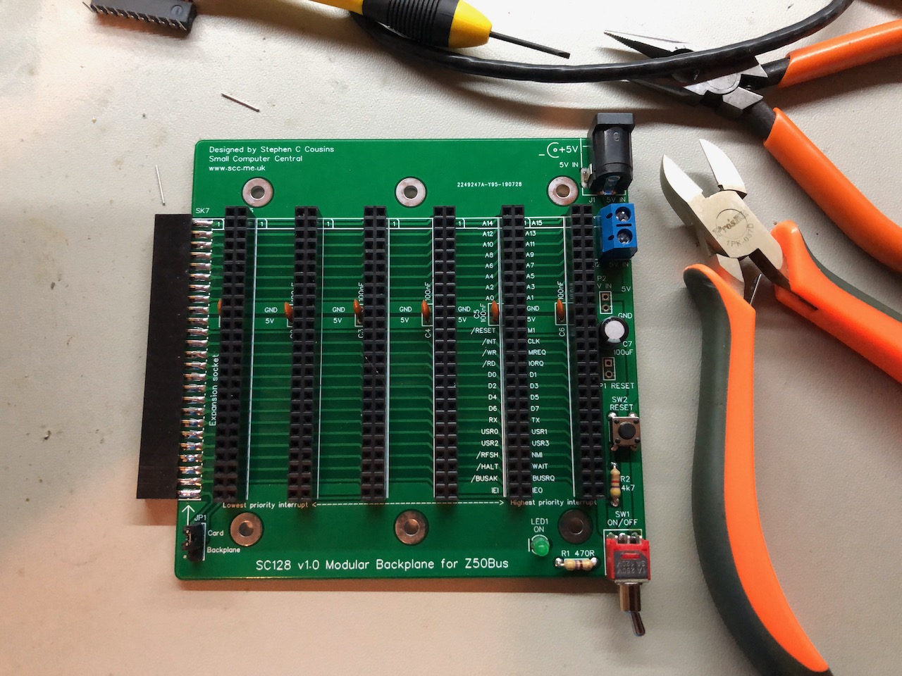
inspired by discussion in the Electronics Wednesday group I have decided to build a retro computer based on the 6502 chip. A couple of weeks back I received a backplane from tindie.com. I’ve completed the assembly and it’s ready to go.
3 Likes
Yesterday I got my PCB’s back from China and have started building the single step/debug board.
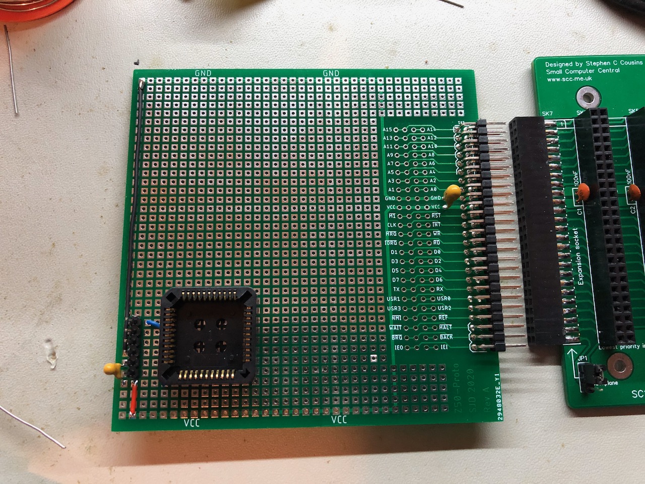
The PLCC socket is for a Xilinx CPLD. I’ve reduced the debug circuitry from 6 or so 9 74’ series TTL chips to a single device.
3 Likes
The schematic below is taken from the 6502 Hardware Manual. It’s the circuit suggested by MOS for debug/single stepping. The functions shown, things like button debounce and RDY signal control have been translated into Verilog and compiled into the CPLD. I will upload the sample code to the MHV GitHub account when I get a chance.

2 Likes
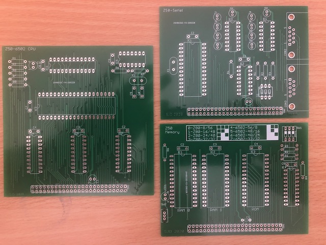
Had a busy day yesterday and managed to complete the last of the 4 board designs I’ve been working on, the processor board.
I sent it to JLCPCB, a big outfit in China. Ordered 5 of each board, 20 in total. Two designs are 75x100mm, two are 100x100mm. The total charge, including DHL 3 day delivery was AUD50.
24 hours after the order was placed the boards are being silkscreened. If you have 30 mins free then https://www.youtube.com/watch?v=ljOoGyCso8s. It’s likely the same factory processing my order.
With any luck they’ll be delivered before next weekend.
3 Likes
The logistics gods have smiled and DHL delivered my boards this afternoon. Now if they can do the same for Toll and my Element14 order I just may have something fun to do over easter.
1 Like
So the parts arrived Wednesday morning and that night I held my own little isolation electronics Wednesday. Managed to assemble the CPU and memory boards without any issues.

When I powered up the CPU board I found that the clock generator was just plain nasty. I have a scope image, but the forum won’t display .TIF files. You’ll just have to take it from me that it was a 2MHz square wave with large spikes before and after the positive square wave signal. Seriously nasty ringing, overtones, I really don’t know why but not what you want to see in a CPU clock.
The oscillator is a standard Pierce configuration. On the breadboard I used a 4MHz crystal, one 74HC00 gate, 1M and 390 ohm resistors and 2x18pF capacitors. The output was perfect!
My PCB version changed two items, the 74HC00 was changed to a 74HCT00 and the crystal went from 4MHz to 2MHz. This was enough to foul things up.
I don’t understand the Pierce oscillator theory very well but I do know that breadboards tend to be capacitive so on a hunch I replaced the 18pF caps with the next available values I had, 33pF. This sorted things out, I now have a good, solid 2MHz square wave feeding the clock divider and CPU.
Now to finish the debug board. Need to get into some CPLD programming and implement the circuit from the 6502 hardware manual.
Looking good. I like the inclusion of the dip switch table, not something you seem much anymore.
Getting a crystal oscillator to start and run well on frequency was always a bit of a trial and error. We often forget how much harder this was 20+ years ago before the silicon designs became so much more tolerant. I think most today would have been less courageous and stuffed a canned oscillator on board!
To be honest, using a canned oscillator never really occurred to me. I’m a hobbyist, not an EE and am completely self trained. Back in the early '80s I had a part time job working for a company that was designing and building its own Z80 based computer systems in a shed in an industrial estate. When I decided to go ‘retro’ this style oscillator was the only way I thought of doing it.
My break with the past is to use 74HCT instead of 74S for the oscillator. In the early '80s CMOS was easily available but we avoided it due to it being 1) slow and 2) static sensitive.
Looking back it’s a little strange. Many of the magazines at the time, Talking Electronics springs to mind, were favouring 4000 series CMOS over TTL in their tutorials. I know which one I’ rather be constantly handling in and out of a breadboard in a hobbyist environment.
Another thing that I decided to do that isn’t quite retro is to use a GAL to reduce the part count. On his last trip to China @spanner888 kindly brought me back a TL866, one of those multi-chip programmers, and after 40 years or so I finally have the ability to program PALs/GALs.
On the CPU board the top chip is an ATF22V10 and I’m using it to replace a bunch of simple and complex logic functions:
- 1 x divide by 2
- 1 x buffer
- some tricky address decoding
It’s probably saved me 4 chips, some of which would have been half used. I did consider using the ‘little logic’ option but then it wouldn’t be retro 
1 Like
Made more progress today. After adding more to the debug board I spent a bit of time going in circles because the signals I was getting out of the CPU weren’t making sense. Turns out the CPU was a dud. Given that I paid $1-2 from China the chances are high these are recycled chips. The replacement worked just fine:
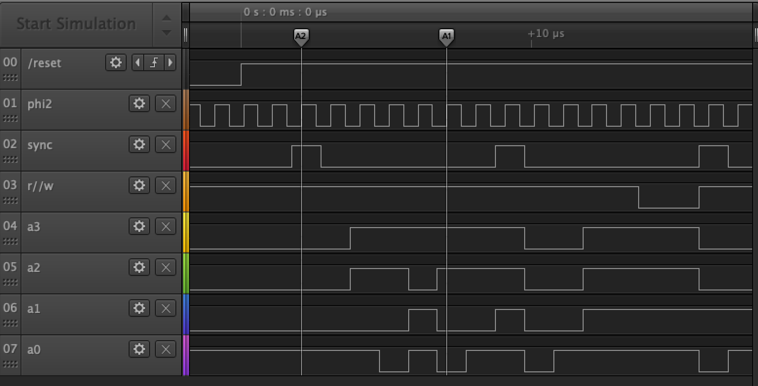
What you’re looking at here is the first couple of cycles following a system reset. The CPU starts executing when /reset goes high (Channel 0). The 6502 uses two clocks, phi1 and phi2. They’re 180 degrees out of phase with much of the interesting external stuff happening on the rising and falling edges of phi2. The sync signal indicates an instruction fetch cycle. r//w indicates a memory read (high) or write (low). The last 4 signals are the low order bits of the address bus.
@mbainrot The 6502 Hardware manual explains this sequence on page A-11. Reset is treated as a special case of BRK. The A2 cursor shows the cycle start, state T0. Cursor A1 shows cycle T5 (fetch from FFFC). This is followed by cycle T6, fetch from FFFD. Memory addresses $FFFC-$FFFD contain the reset address i.e. where to start executing from following a system reset.
After the T6 cycle things will just run wild as I have not yet installed a ROM. Most likely the system will read bytes FF and FF ($FFFF) and attempt to start executing from there.
Next step, a simple ROM to put the CPU into a hard loop.
1 Like
Todays progress went fast and then slow. I started out working on a simple test program, nothing complicated, just zero a couple of registers and then stick itself into an endless loop. This was more a test of the tool stack than the hardware.
I’m using the cc65 stack. It’s a C compiler, assembler and link loader targeted at the 65xx family. It will generate code for the Apple 1/2, C64, Acorn etc.
A couple of weeks back I’d managed to set up a basic assembly sequence using the make utility. The cc65 suite is more complicated than the regular old assemblers I’m used to. Because it puts C into the mix it generates relocatable object files rather than a single, absolutely located binary. It takes a bit of tweaking to get it to generate a ROM binary image. If you’ve worked in assembly you’re probably used to the .ORG directive (setting an absolute location). The ca65 assembler sort of recognises the directive but then proceeds to ignore it. Weird I know but it really wants to create relocatable code. You have to tweak the linker to get things where you want.
Once I got a usable ROM my attention then turned to the memory card (see above). This project is repurposing an existing bus, Z50, which is aimed at the Zilog Z80 chip. I am trying to design a generic memory card however there is a key difference between the Z80 and 6502 chips. The Z80 wants its ROM located at the bottom of memory, address $0000 is where is starts from during reset. The 6502 works the other way, it wants its ROM chip at the top of memory, loading its reset vector from $FFFC.
With this mind my memory card is designed to work with both processors. The 3 way DIP switch (red block) selects one of eight possible memory maps, 4 per processor. This requires some “interesting” address decoding and I’m using a Generic Array Logic (GAL) chip to perform the memory decode. Google “atmel atf16v8b datasheet” if you’re interested.
The slow part of the day was spent trying to get the WinCUPL tool to work in Win 8 x64. The bottom line is that it works just well enough to keep you trying. Once I spun up a Win7 x32 VM it was stable and I was able to progress.
Did not get the memory card working properly today but have got the GAL toolchain stable and productive.
Hi all,
have been chipping away for the last two days on the debug board. The single step functions, single cycle and single instruction, appear to work but I’m a little perplexed by the way the Hardware Manual describes the single cycle function and WRITE cycles.
I’ve uploaded the CPLD Verilog source here. Am still unable to determine the difference between the way the text on pg. 124 differs from the circuit on pg. 125. The text suggests that it ‘skips’ over WRITE cycles when a single step encounters one. The way the circuit is shown, the bottom right FF resets for WRITE cycles and this disables the single cycle button. It takes a button press to reset the ‘write’ FF.
If any of you have experience with this I’d appreciate your input.
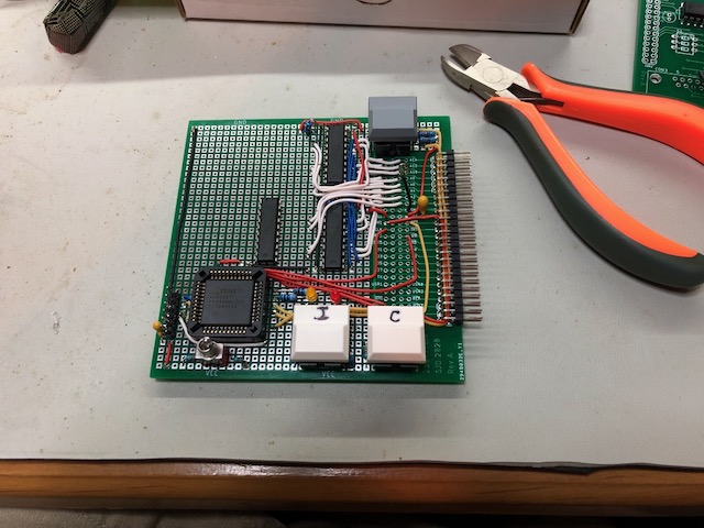
Progress-wise the CPLD is probably done, ignoring bugs. I now need to spend time working on the latches, so that the address and data bus values are displayed. My intention is to add an 8 character, 7 segment display, one of the cheap Chinese boards based on the MAX7219, I’ve seen a few kicking around the electronics Wednesday group so I hope you know what I’m talking about.
The 3 large chips in the photo above are 74HCT373 latches, 16 bits for the address bus (white and blue wires) and 8 for the data bus (not wired up yet).
I plan on adding an Atmel Attiny2313 processor to operate as the display multiplexer/driver i.e. read the
latches one by one and then send data to the MAX7219 over SPI.
I’m hoping that this additional detail will show me what’s going on with the processor. I’ve had one clearly blown 6502. The second is responding to the single step pulses but the address bus isn’t doing what I expect, wrong values on the address bus at critical times. Maybe another dud 6502 chip. I may have to pay some real $$, rather than rely on second hand stuff from Aliexpress ![]()
If you have experience with the 6502 and it’s write cycle behaviour I’d really appreciate your input.
Cheers,
SteveD
Gave the circuit a good bit of attention tonight, working it over with the logic probe. Now that the debug board is working reliably I can step one cycle at a time into the CPU/ROM cycle. I can see that that the chip reset does what it’s supposed to do and that the load of the reset vector from ROM is happening. The ROM is decoding correctly and it outputs the correct values. These values make it back to the CPU.
There appears to be a problem with the CPU itself. Once the reset vector loads it begins the next instruction fetch from a location that just isn’t right i.e. should fetch from $F800 but next fetch is from elsewhere.
I’ve gone through the 6500 Hardware Manual and everything checks out. The data bus voltages are well above their thresholds and the values are correct. The only conclusion I can make at this point is that the CPU is fouled up. Given that I bought them as Chinese surplus for very little $$ I can only guess that I got what I paid for.
Have ordered some genuine new W65C02 parts from Mouser. They may take a few days to get here. Will post again once I am able to debug with new components.
The new processor, a WDC65C02, turned up Friday. Have hacked things to the point where the CPU card, ROM memory and serial are all working.
My baby’s first words:
![]()
3 Likes
How exciting! What next?
Do you have software for your computer? I have a 6502 computer which has software in ROM (4 of them) running basic. It is socketed so you may be able to attach to your kit. It accepts 300 baud serial (mostly used for cassette save/load).
Thanks @eyal, very kind to offer. I’ll keep it in mind.
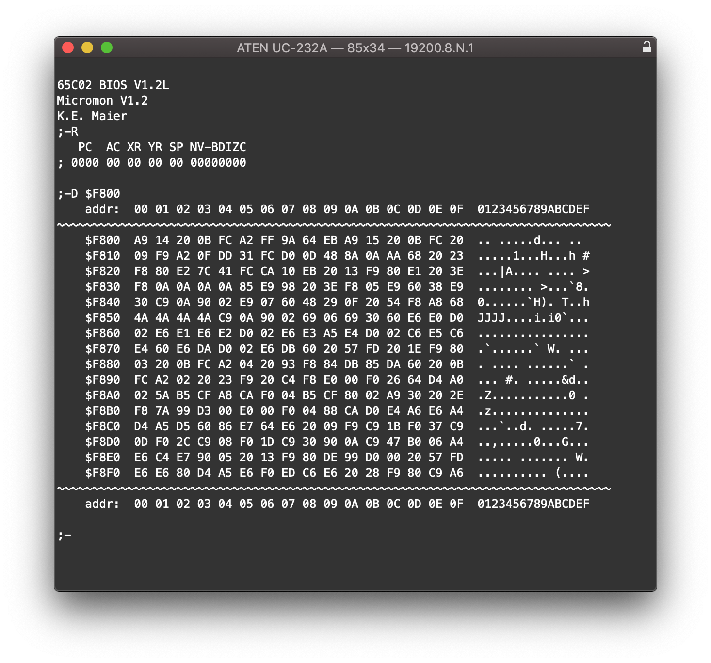
Right now I’m trying to get this open source monitor to work correctly with my hardware. I’m getting data out, which means the RAM must be good because the monitor uses interrupts and RAM buffers. Unfortunately it’s not responding to input.
The monitor code is VERY well written assembler but it’s still assembler and it can take a bit of parsing to follow it through.
Well that didn’t take long. After finding the relevant section in the code it became clear that the serial chip just wasn’t receiving data. After checking the receive data line (ok) I checked some of the other modem controls, one wasn’t set where it should. After tying it high everything just worked. Brilliant!
I take no credit for the monitor code, it was all Kevins work. I just had to tweak a few settings to get it working with my memory map and assembler.
2 Likes
Hi @sjdavies - have you had any time to progress your project?