This is in reference to the discussion we had on Discord last night. I don’t know if Dr4t is on the forum?
I plugged the numbers for JLCPCB’s JLC2313 layer stackup into their calculator, Saturn PCB toolkit (my personal favorite), and some random webpage that came up with a google search. Results below:
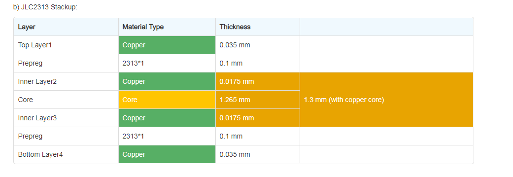
The stackup numbers from JLCPCB:
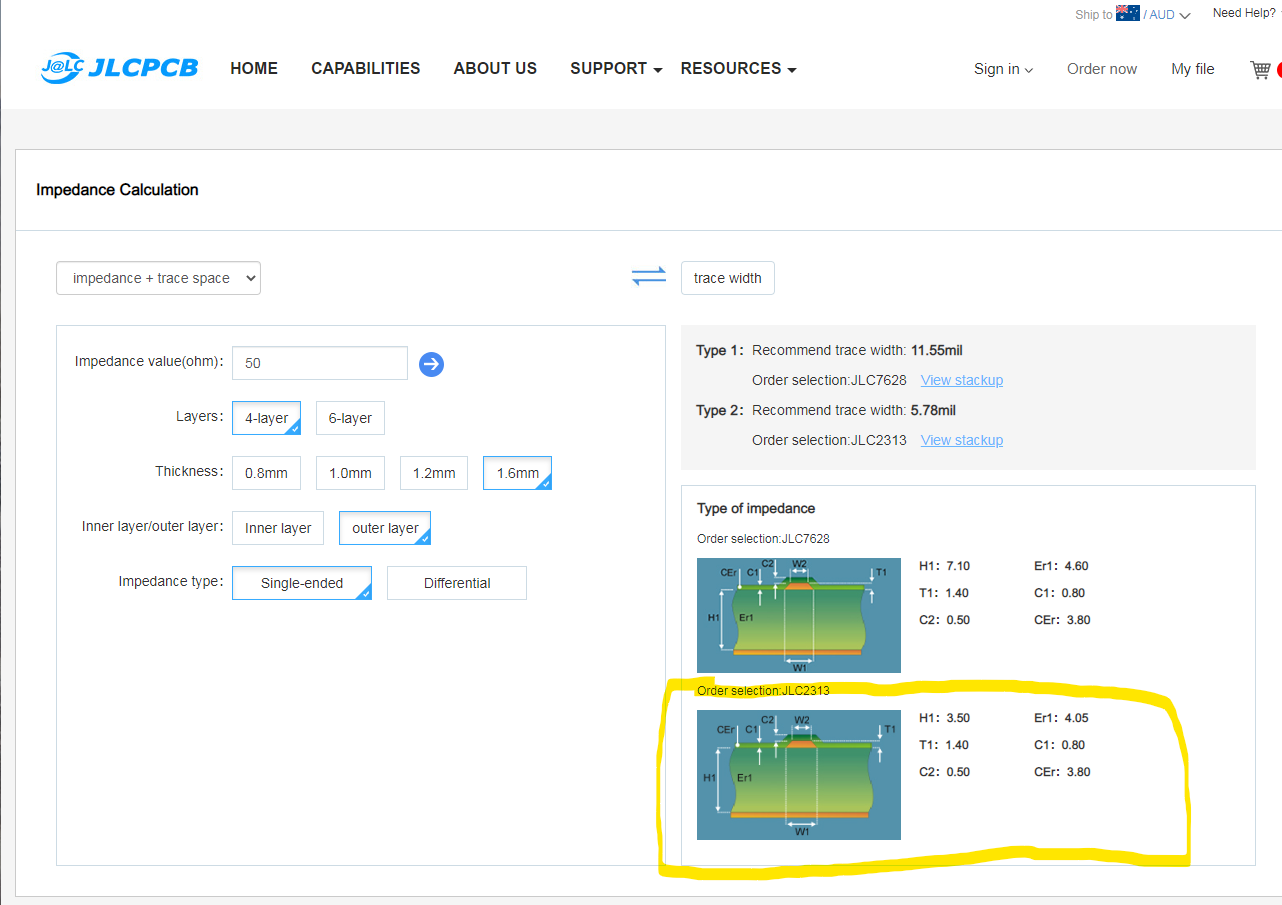
JLC’s calculator:
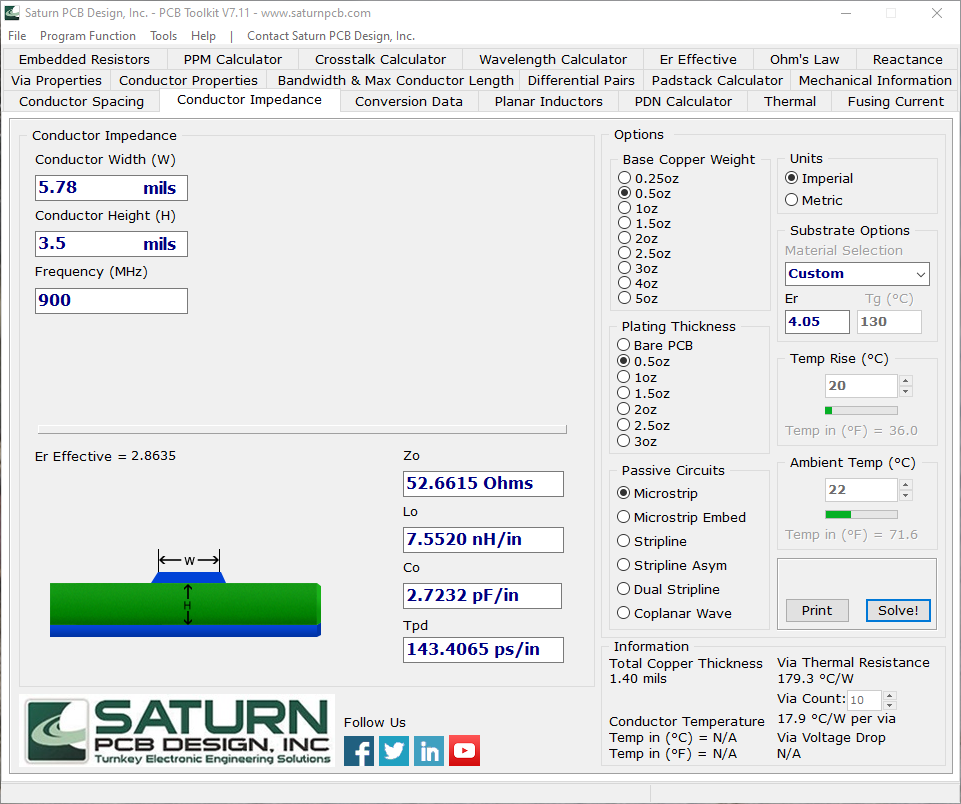
Saturn toolkit:
Other:

Not sure what PCB he is targeting, but the basic 4-layer JLC2313 results look consistent to me. ~0.15mm trace width @ 50ohms (6 thou in the old language). This is roughly what I remember from designs I’ve done in the past as well.
Using JLC’s other impedance controlled stackup 7628, due having double the thickness dielectric layer between layers 1 & 2, results in roughly double the track width and becomes unwieldy with small parts. Great for running between larger connectors, inductors and the like though (e.g. lower frequency work).