Another FPGA project

I have to apologise for not being more social with the Discord evenings.

I’ve started toying around with implementing the algorithm in the following paper in an FPGA:

Mostly because I’ve never had the need/opertunity to do much with DSP and FPGAs.

I understand that most won’t have access to IEEE, nor will have much interest in power system synchrophasor estimation. Which is fair enough, but there’s some interesting challenges in the algorithm.

The basic constructs of the algorithm are as follows:

  • Collect typically 1.5 line cycles of samples with GPS timestamp
  • Perform two vector multiplication and accumulate operations on the sample set with a set of coefficients that correspond to the predicted line frequency.
  • Calculate the arctan of the output of the previous step to get the phase.
  • Calculate the frequency from the difference in phase between the previous cycle and the current cycle.
  • This cycle is repeated to update the predicted frequency until it converges, or a max number of iterations are achieved.

This isn’t a difficult algorithm to implement in software (hence it’s been quite popular), however it needs quite a bit of processing grunt to achieve realtime (think RPi) which is difficult with the requirement for microsecond timestamping. If it can be done in a smallish FPGA, it will significantly reduce the cost and complexity of current implementations I’ve read and been involved in previously.

So the first part, hooking up an ADC and streaming into a cyclic block ram buffer is pretty straightforward.

The second part, the vector multiplication with a varying set of coefficients is the first challenge. This needs around 3-400 multiplication/accumulate operations per update, with a unique set of coefficients for each frequency interval. E.g. 50.01Hz, 50.02Hz etc. So bounding to 45 to 55 Hz with 0.01Hz resolution, that’s 1000 coefficient sets.

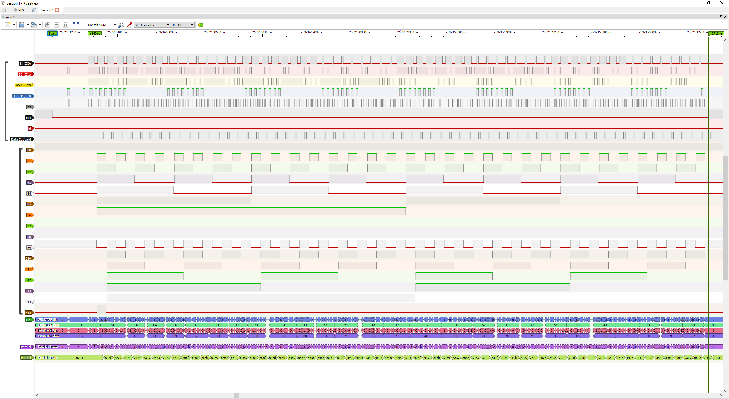
That works out to be around a couple of MB of constants, so it’s clearly going to be external to the FPGA. I’ve toyed around with a few ideas and settled on using SPI Flash memories that support 100MHz Quad-SPI mode, as they’re dirt cheap (used in ESP8266 modules), and can approach 50MB/s read rate using the constant Q-SPI read mode.

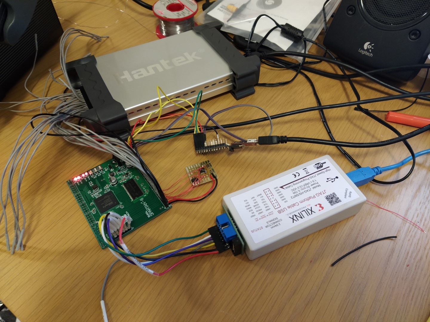
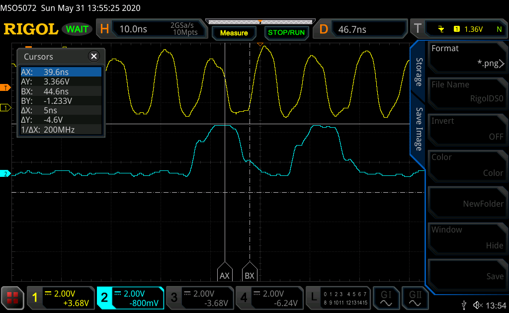
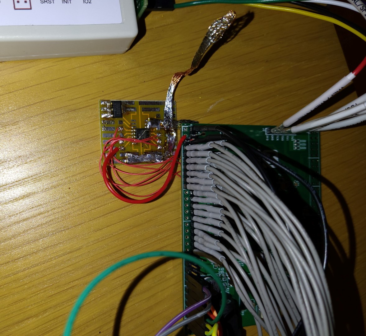
I have a controller built that I’ll put into github once it’s cleaned up a bit. So far I have it working up to about 50MHz SPI clock, but signal integrity and a fairly naive implementation is holding it back. Need to design a proper PCB and adjust the controller design to put the input registers into the IO blocks to reduce the propagation delay. This could be quite a useful little block in itself for other projects.

For those that haven’t used FPGA’s much, one of the really nice things is the ability to route signals to any pin for in system programming/testing. In the pic below I have an Ardunio’s SPI bus hooked up to a few other pins on the FPGA, and a project that just links the Ardunio up to the SPI flash for programming it.

The rest of the processing pipeline I think should be doable, so I think it’s time to make a PCB for the project.

Ok that’s more than enough for one post…

2 Likes

Hi Derryn,
I’ve been digging through an old online course in an attempt to understand what it is you’re trying to do here.

Based on your description it sounds like you’re building an engine to compute a series of inner products between the power line signal, nominally 50Hz, and reference sinusoids, 45-55Hz in 0.01 Hz steps i.e. which of the 1000 possible frequency values is the ‘best’ match for the current power line signal.

Is this correct?

Pretty much, I’ll pm you a link if you want to have a look. It is Least Error Squares curve fitting to a reference wave, of a guessed then updated frequency.

Any attempt I make to explain the math behind it will make a mess of it :slight_smile:

But the outcome is we want the frequency, phase and magnitude, updated every cycle (or half cycle), including in the presence of noise and waveform distortion.

Thanks for the paper, interesting but the terminology and maths is a little beyond Me ATM.

Found this useful https://en.m.wikipedia.org/wiki/Phasor_measurement_unit

Yeah I’m pretty much the same TBH. But as I’ve proven, you don’t need to fully understand the maths to implement it and have it work well.

I used some DSP slices from the Artix 7 for my Hammond organ project. There are some minor improvements in 7 series slices over S6. I think overflow handling may be one of them. Could be worth a look.

I would have liked to use a 7 series for this and get away from ISE in a VM. But this is looking like it’ll easily fit in a XC6SLX9, which is $8 at the moment. The cheapest 7 series device I’ve found, the XC7S6, is still 3x that price and are all BGA only.

No big deal for a few of, but it would be nice to keep the component cost low for this application.

I’ve added the project to github. There’s the module itself and a test harness.

I’ve put all the qspi into IO DDR registers which actually cleaned the state machine up quite a bit, as it’s then simple to define which clock edge things should happen on.

Also now working well @100MHz qspi clock, which is kind of a surprise! More below.


Here’s an example of the timing for a 64, 16-bit word read, which will probably be along the lines of what I’ll be needing to do. In this there’s ~150ns overhead for transmitting the address, M-code bytes (control bytes) and required dummy bytes at the start, then a 4-bit nibble every 10ns. So overall 2.7us for the 128byte read.

So I’ve looked at the clock and spi-flash response signal on the scope using spring ground clip. These are basically a little spring that you put on the probe tip and use to ground the probe instead of the long lead to eliminate the the lead inductance.

Here’s the trace of the clock (from the FPGA) and one of the data lines (while driven by the spi flash).

So obviously this isn’t the cleanest, passive probes, 350MHz scope bandwidth and all that. But I have markers on two edges that correspond to the falling edge where the data should be shifted out and the rising edge where the fpga will register the data. Obviously this is getting pretty close, so may need to use some delay element (which I think is built into the IO blocks) to better align the clock with the eye opening.

Having said all that, the test harness is checking the received data from the flash (a simple count sequence) and it’s been running for a couple of hours with zero bit errors, so I’m calling that a success.

Cool!

Is this running with the memory mounted on the breakout board in photo 1?

Re analyser trace:

  1. signal clk appears non-periodic. Is this due to aliasing (100MHz signal sampled @ 400MHz)?
  2. B15-B0 appear to be counter outputs and out of phase. Assume they control coefficient memory loading. Are the coefficients complex numbers?

I’ve seen eye diagrams before but don’t fully understand them. Have read that they’re related to jitter. Does your ‘scope provide a way to measure it?

It is the same breakout board, however I’ve used desoldering braid to make a bit of a perimeter ground plane and solder it in close to the fpga board. Far from perfect, but much better than having a single ground wire. Still kind of surprising to get good enough signal integrity for this to work.

  • Clock signal, not quite sure in that screen grab. Obviously it’s not real, but it shouldn’t be the logic analyser, as @400Msps there should be a least one sample high and low per clock. I’d say it’ll be the rendering by sigrok/pulseview. Otherwise a fabulous piece of software though, it’s turned a cheap chinese LA with unworkable software into something really useable!

  • Yeah sorry I should have explained that better. The bus on the B channel, along with the Data Out Valid signal are a parallel bus that’s the output of the vhdl module (i.e. output from the flash memory). It’s just counting as that’s what’s programmed into the flash memory. It seemed like the easiest thing with plenty of transitions to check with the fpga (i.e. just implement a counter to check the flash output against.) Hope that makes sense!

That paper is fairly dense for non-math types. Am trying to figure out the memory calculation 4 x 52 x 2 x 2. Is it:

  • 4 - size of coefficient
  • 52 - frequency steps
  • 2 - first two lines (real/imag)
  • 2 - ??

Given the iterative algorithm are you expecting to perform a variable number of calculations or in true fpga style calculate everything and just select the best result?

I assume that the transformations on A can be performed at design time yielding the coefficient matrix.

Yeah it’s a bit interesting that little bit of the paper, they haven’t fully explained how that got to that number and to be honest I’m not totally convinced a mistake hasn’t been made. Although I could certainly be wrong.

In particular with the 52x, because 52 in there example will be the other side of the pseudo-inverse matrix. The length that needs to be stored for the filter is relative to the sample rate.

The way I see it for the implementation I’m attempting will be:
3B - size of the coefficient - It’ll be fixed point and probably 24bit will be plenty
x41 - Number of samples in the filter window - the paper specifies 1.5 line cycles. At the moment I’m thinking of 2ksps, as I’ve used 1.5ksps before and it’s been fine, plus it’s a even divider of the ADC. So 1.5*(2000/50)+1=41.
x2 - As you’ve said, real/imag, or another way of looking at it is in-phase and quadrature.
x1000 - 45 to 55Hz @0.01 steps.

So that’s 246kB.

I imagine the extra 2x will be for 50Hz and 60Hz systems. It’s common on these devices to be switchable between regions. But I could be wrong, they may have some other things going on.

You’re completely right about pre-calculating the pseudo-inverse of A, and storing the rows needed. That’s what makes this algorithm relatively easy to implement, it just needs some reasonable storage.

As for the iterative approach. While it makes some sense in software to stop when you’ve found the solution (or hit max iterations), in the FPGA just running a fixed number of iterations seems simpler and should need less logic. I don’t think there’ll be enough time to calculate the phase and frequencies of all frequencies without larger FPGA (given there’s 1000 possible frequencies).